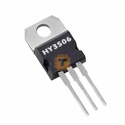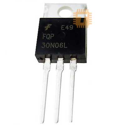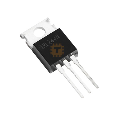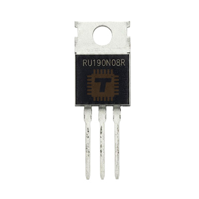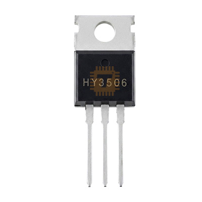
Original HY3506 N-Channel Enhancement Mode MOSFET
Price in Sri Lanka
FETTransistors and Diodes
Tronic.lk

Rs 260
In stock
Updated 01 Nov 2026
Opening hours
Closed now
- Monday09:00 - 19:00
- Tuesday09:00 - 19:00
- Wednesday09:00 - 19:00
- Thursday09:00 - 19:00
- Friday09:00 - 19:00
- Saturday09:00 - 19:00
- SundayToday09:00 - 19:00
Search for it on
Description
The Original HY3506 / HY3506P N-Channel Enhancement Mode Power MOSFET (60V / 200A / TO-220) is an ultra-high-current, low on-resistance power MOSFET engineered for high-efficiency DC power switching, high-current motor control, synchronous rectification, and battery management systems. Utilizing advanced trench-gate processing technology, it delivers exceptionally low on-state drain-source resistance ($R_{DS(on)}$ typ. 2.4 mΩ to 2.8 mΩ), dramatically minimizing conduction losses ($I^2R$) and thermal buildup during heavy current delivery. Housed in an industry-standard through-hole TO-220 package, it offers a drain-source breakdown voltage of 60V with continuous drain current handling up to 200A (silicon limited) and 100% tested avalanche ruggedness. The HY3506 is widely utilized in electric vehicle (EV) speed controllers, e-bike/scooter motor drives, high-power DC-DC converters, solar inverters, and heavy-duty DC electronic switches.
Specifications
- Part Number / Model: HY3506 / HY3506P
- Transistor Polarity / Type: N-Channel Enhancement Mode Trench Power MOSFET
- Package Type: TO-220-3L (Through-Hole Power Package with Metal Mounting Tab)
- Drain-Source Breakdown Voltage ($V_{DSS}$): 60 V (Min. at $I_D = 250\text{ μA}$, $V_{GS} = 0\text{V}$)
- Gate-Source Voltage ($V_{GS}$): ±20 V Max.
- Continuous Drain Current ($I_D$):
- At $T_C = 25^\circ\text{C}$: 200 A (Silicon limited) / Typ. 120A–140A (TO-220 lead package limited)
- At $T_C = 100^\circ\text{C}$: Approx. 140 A
- Pulsed Drain Current ($I_{DM}$): Up to 800 A ($t_p \le 10\text{ μs}$)
- Static Drain-Source On-State Resistance ($R_{DS(on)}$):
- Typ. 2.4 mΩ (at $V_{GS} = 10\text{V}$, $I_D = 75\text{A}$)
- Max. 2.8 mΩ (at $V_{GS} = 10\text{V}$, $I_D = 75\text{A}$)
- Gate Threshold Voltage ($V_{GS(th)}$): 2.0 V to 4.0 V (Typ. 3.0 V at $I_D = 250\text{ μA}$)
- Total Power Dissipation ($P_D$): Up to 260 W (at $T_C = 25^\circ\text{C}$)
- Single-Pulse Avalanche Energy ($E_{AS}$): Approx. 1350 mJ ($L = 0.5\text{ mH}$, $V_{DD} = 30\text{V}$)
- Total Gate Charge ($Q_g$): Typ. 165 nC to 185 nC (at $V_{DS} = 30\text{V}$, $V_{GS} = 10\text{V}$, $I_D = 75\text{A}$)
- Input Capacitance ($C_{iss}$): Typ. 9100 pF (at $V_{DS} = 30\text{V}$, $f = 1\text{ MHz}$)
- Output Capacitance ($C_{oss}$): Typ. 1100 pF
- Reverse Transfer Capacitance ($C_{rss}$): Typ. 750 pF
- Body Diode Continuous Forward Current ($I_S$): Up to 200 A
- Body Diode Forward Voltage Drop ($V_{SD}$): Typ. 0.85 V (Max. 1.2 V at $I_S = 75\text{A}$, $V_{GS} = 0\text{V}$)
- Thermal Resistance (Junction-to-Case, $R_{\theta JC}$): 0.58 °C/W
- Thermal Resistance (Junction-to-Ambient, $R_{\theta JA}$): 62 °C/W
- Operating Junction & Storage Temperature ($T_j$, $T_{stg}$): -55°C to +175°C
- Pinout Configuration (TO-220 - Front View, Pins Facing Down):
- Pin 1: Gate (G)
- Pin 2: Drain (D) - Connected internally to Metal Mounting Tab
- Pin 3: Source (S)
- Mounting Tab: Drain (D)
Features
- Ultra-Low On-Resistance ($R_{DS(on)} \le 2.8\text{ m}\Omega$): Greatly reduces conduction power losses, enabling cool and highly efficient operation under heavy current loads.
- High-Density Trench Technology: Delivers optimal switching speed, extremely low conduction resistance, and exceptional thermal ruggedness.
- High Avalanche Energy Handling (100% $E_{AS}$ Tested): Provides superior resilience against inductive voltage transients and unclamped inductive switching (UIS) typical in heavy motor drives.
- Standard High-Power TO-220 Package: Through-hole footprint mounts easily onto aluminum heatsinks, chassis cooling plates, or custom cooling assemblies.
- Extended Junction Temperature Rating (+175°C): Ensures dependable, long-term continuous operation under extreme thermal and electrical stresses.
Common Applications
- High-Power DC Motor Controllers: PWM speed drivers and H-bridges for electric bikes, scooters, golf carts, winches, and robotics.
- Synchronous Rectification & SMPS: Secondary-side low-loss rectification in high-power industrial and telecom switch-mode power supplies.
- High-Current DC-DC Converters: Buck and boost power conversion stages in solar charge controllers (MPPT) and high-current step-down regulators.
- Battery Management Systems (BMS): Solid-state electronic disconnect, overcurrent, and short-circuit protection for 24V, 36V, and 48V Lithium battery packs.
- Power Inverters & UPS Systems: Primary-stage low-voltage DC switching legs for 12V/24V/48V pure sine wave and modified sine wave inverters.
- High-Current Solid-State Relays: Contactless switching for high-amperage automotive accessories, solenoids, and DC actuators.
Usage Tips
- Heatsink & Thermal Mounting (Crucial): At continuous load currents above **10A to 15A**, mounting the TO-220 package to an appropriately sized aluminum heatsink using thermal compound is mandatory. For continuous currents exceeding 35A–40A, active fan cooling is strongly recommended.
- Tab Electrical Isolation: The metal mounting tab is **internally connected to Pin 2 (Drain)**. If multiple MOSFETs share a common grounded heatsink (such as in an H-bridge or half-bridge configuration), use silicone insulating pads (Sil-Pads) or mica insulators along with insulating shoulder washers on the mounting screws.
- Gate Drive Voltage: The HY3506 is a standard-gate MOSFET requiring a **full gate-to-source drive voltage of $V_{GS} = 10\text{V}$ to $12\text{V}$** to fully saturate and achieve its minimal $2.4\text{ m}\Omega$ on-resistance. Do not drive the gate directly with 3.3V or 5V logic signals from microcontrollers (Arduino/ESP32); always use a dedicated high-current gate driver IC (such as the TC4420, IR2104, or TC4427).
- Driving Large Gate Capacitance: Due to its substantial input capacitance ($C_{iss} \approx 9100\text{ pF}$), use a low gate series resistor (typically **4.7Ω to 10Ω**) to maintain fast switching rise/fall times and minimize switching losses. Always place a **10kΩ pull-down resistor** between Gate and Source to prevent spurious turn-on during power-up.
- Inductive Load Flyback Protection: When switching inductive loads (motors, relays, or solenoids), place an ultra-fast recovery or Schottky freewheeling diode across the load, or add an RC snubber network across Drain and Source to suppress inductive voltage spikes below the 60V limit.
Frequently asked questions
What is the price of Original HY3506 N-Channel Enhancement Mode MOSFET in Sri Lanka?▾
The current price of Original HY3506 N-Channel Enhancement Mode MOSFET in Sri Lanka is Rs 260 at Tronic.lk.
Is Original HY3506 N-Channel Enhancement Mode MOSFET available in Sri Lanka?▾
Yes, Original HY3506 N-Channel Enhancement Mode MOSFET is currently in stock at Tronic.lk in Sri Lanka.
Where can I buy Original HY3506 N-Channel Enhancement Mode MOSFET in Sri Lanka?▾
You can buy Original HY3506 N-Channel Enhancement Mode MOSFET in Sri Lanka at Tronic.lk. Visit 37left.lk to compare prices across multiple shops and find the best deal.
Loading...